Photo of the module in a perspex frame,
00/10/20
Sensor I-V measurement of the module, at 18 deg.C, no ASIC power, readout of analog current meter,
00/10/20
Default setting: Vdet=150V, FEbias(Ipre)=220uA, FEshaper(Ishpr)=30uA, Comp=0, Edge=0, trimR=0
Low-vol and HV were supplied with bench power supplies
Module was measured in the thermobox with air cooling of 18 deg.C. Temp of hybrid was about 30 deg.C
Strobe delay scan with Comp=1, Edge=1, no trim, for Vth~2fC and Vcal=40mV,
00/10/20
Strobe delay at 20% of plateau, delay=38
Timewalk of link0, and
link1,
with Comp=1, Edge=1, no trim, for Vth~1fC, (ignore the fitted curves for the moment),
00/10/20
Trim scans: with default Ipre/Ishpr=220/30uA, for 2fC Vcal,
trimR=0,
trimR=1,
trimR=2,
trimR=3,
best target (min. rms) at 140 mV,
trim files (
trimR=0,
trimR=1,
trimR=2,
trimR=3),
mask files (
trimR=0),
00/10/20
with Ipre/Ishpr=220/20uA, for 2fC Vcal,
trimR=0,
trimR=1,
trimR=2,
trimR=3,
best target (min. rms) at 125(trimR=0) and 140(others) mV
trim files (
trimR=0,
trimR=1,
trimR=2,
trimR=3),
mask files (
trimR=0,
trimR=1,
trimR=2,
trimR=3)
Response curves: with default Ipre/Ishpr=220/30uA, trimR=0,
q=0-8fC polynomial fit including all points of link0,
link1,
and data files of
link0,
link1,
00/10/20
data files of q=2,3fC linear fit of link0,
link1,
00/10/20
Matrix scans: Ipre=100,150,200,250uA, Ishpr=20,30uA, with trimR=0 (of 220/30),
noises and gains of link0, and
link1,
and
data files of link0,
link1,
00/10/20
Uniformity of thresholds of
Ipre/Ishpr=220/30 link0,
link1,
(trimR=0 of 220/30) and
Ipre/Ishpr=220/20 link0,
link1,
(trimR=0 of 220/20),
00/10/20
fractional uniformity at 1fC with the
q=2,3fC linear fit gains
Noise scans of no trim, trimR=0, and single s-curves of no trim link0, link1, trimR=0 link0, link1, 00/10/20
Digital current (Idd) as a function of threshold, trimR=0, 00/10/20
Measured in a climate box at -15 deg.C forced air flow.
Module in a H8 test box with lid closed.
I-V curve of the module at -15 deg.C
Vcc=3.50V, Vdd=4.00V ON, Hybrid temp(thermistors) at about +3 deg.C
Detector file: .det file (delay=34), updated 01/3/19
Trim scan,
and trim and mask files: .trim file,
.mask file
Noise scan with EDGE=0 and COMP=0,
S curves of link0 and
link1
Response curves, 01/3/19
Testsheet of k3112 module,
00/0821
A trim file for Q=2fC and Vth=200 mV
and the mask file,
00/06/22
Testsheet of k3111 module,
updated 00/0821
Comparison of gain and noise with 2,3fC linear fit,
00/08/21
Comparison of gain and noise with 0,2,3fC linear fit,
00/08/21
A photo of the k3111 module (jpg)
k3111 hybrid is made of the version 3 Cu/Polyimide hybrid on a polymer-coated Carbon-Carbon bridges glued conductively to the hybrid pads (AGND) conneced to the chips. This round of chip batch had larger trim variations. The chips were arranged such that the chips with least untrimable channels were in the middle (S2, S3, S10, S11) and the worst ones were in the end of chain (E5, E13, S4, S12).
Operation condition of the module: FEbias current=267 uA, FEshaper current=30 uA, Vcc (sense, i.e., at support card) = 3.50 V, Vdd (sense) = 4.00 V, Vbias (detector) = 150 V, Leak current = ~ 0.8 uA, cooling at 18 deg.C in a climate box.
Trim scans with Vcal=20 mV=2 fC. Out of the scan, Vth=200 mV was chosen to set trims. This is because the slope of trim step is steep in the low trim regions, which means the rms of the threshold uniformity is not good. Above 200 mV, the slope of trim step is uniform, yet the number of untrimable channel is stable. This left 1461 trimmable (or 75 untrimmable) channels. Trim file of 2 fC=200 mV. Noise pedestals (=offsets) with the trim file of 2 fC=200 mV, obtained with the Edge=off, Comp=x1x condition. Threshold uniformity at 2 fC of link0 and link1.
Noise occupancy scans in upward and downward scans, between 0 and 200 mV threshold in a step of 2.5 mV. S-curves of all channels of link0 and link1 of the upward scan, and link0 and link1 of the downward scan.
Gains and noises were calculated from a linear fit of the 3 points of 0, 2, and 3 fC threshold scans. Response (top-left quad.), Output noise (bot-left quad.), Gain (top-right quad.) and Input noise (bot-right quad.) of 6chips of link0, and those of link1. Fit parameters, offsets, gains, noises are listed for link0, and link1.
Another response curves of the charge points between 2 and 8 fC are plotted for link0, and link1 with a second-order polynomial. Fit parameters, offsets, gains, noises of the 2-8 fC fits are listed for link0, and link1.
Noise occupancy scan with Edge=ON and Comp=01X, Peak positions can be read from the Gaussian fit.
Response curves with Edge=ON and Comp=01x of link0, and of link1. Data list of link0, and link1. Noise values are smaller in the Edge=ON mode than Edge=OFF mode. 2000/5/24
Hybrid only (without sensors): noise scans of link0, and link1, 00/05/05
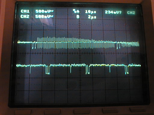
Time-walk measurements of the 12 chips module, and a list of parameters of a fit function. An inverse-sqrt curve, f(x)=p0+p1/sqrt(x-p2), was a good fit function. 00/05/25
The k3104mod module has a long history. The hybrid is the version 3 on metalized Carbon-Carbon bridges. ABCD2T chips were from the same batch of the "Mod0". The module was made by using temporaly components: very early prototype of TPG baseboard with AlN facings and ATLAS97 detectors, because of the lack of latest components. Bearing in mind to replace the detector-baseboard assembly in future, the hybrid was "screwed" on the baseboard, rather than glueing. After turn-on the power, the module performed inferior to "Mod0": one sick chip in the trim DAC step, larger detector leakage current, etc., and in addition, exhibitting small global instability in one 6 chip side of hybrid of about 20 mV band in threshold around the noise peak (with Edge=ON mode). Despite number of trials to cure the problem, no fundamental prescription was found. During the struggle, one chip was died due to lack of cooling; the detector leakage current was increased time by time and at the end more than 40 uA at 18 deg.C cooling. After all these poor conditions, the module was decided to go for a major surgery: dismouting the hybrid from the module, replacing the sick and dead chips, and assembing into the latest detector-baseboard assembly. After the surgery, the new module, "Mod2mod" (or k3104mod), the hybrid being glued on the baseboard this time, revived!! The module is as stable as "Mod0".
Following data were taken for the "Mod2mod" with the operation condition of the module: FEbias current=267 uA, FEshaper current=30 uA, Vcc (sense, i.e., at support card) = 3.50 V, Vdd (sense) = 4.00 V, Vbias (detector) = 100 V, Leak current = ~ 0.6 uA, cooling at 18 deg.C in a climate box, Edge=OFF and Comp=X1X, if otherwise said.
Trim scans with Vcal=20 mV=2 fC. Trim set to Vth=200 mV, which left 1518 trimmable (or 18 untrimmable) channels. Trim file of 2 fC=200 mV and Mask file. This trimming was done at the stage of hybrid. The trim file was used temporarily (lack of time). Threshold uniformity at 2 fC of link0 and link1 of the module.
Noise occupancy scans in upward and downward scans, between 0 and 250 mV threshold in a step of 2.5 mV. S-curves of all channels of link0 and link1 of the upward scan, and link0 and link1 of the downward scan. There was no hint of discontinuity in a single chip.
Gains and noises were calculated from a linear fit of the 3 points of 0, 2, and 3 fC threshold scans. Response (top-left quad.), Output noise (bot-left quad.), Gain (top-right quad.) and Input noise (bot-right quad.) of 6chips of link0, and those of link1. List of fit parameters, offsets, gains, noises of link0, and link1.
Response curve of the charge points between 2 and 8 fC of link0, and link1, with a second-order polynomial fit. List of fit parameters, offsets, gains, noises of the 2-8 fC of link0, and link1.
Noise occupancy scan with Edge=ON and Comp=01X, Peak positions can be read from the Gaussian fit.
Response curve with Edge=ON and Comp=01x of link0, and of link1. Data list of link0, and link1. 2000/5/26
"Mod0" uses "metalized" Carbon-Carbon bridges glued conductively to the Cu/Polyimide hybrid which has conducting pads (AGND) underneath the chips.
Associated...
(Preliminary!) Double-sided ABCD2T barrel Cu/Polyimide module at KEK, revised, 99/11/27
(6) Noise and charge injection scans with the FE "shaper" current of 10 uA, 99/4/7
The previous measurements, (1) - (5), were done with the FE "shaper" current of 18 uA.
New data were taken with the FE "shaper" current of 10 uA.
The "bumps" were gone!
Also, the 1st and the 2nd chips were quiet!
The new scans were, then, made with the 1st and the 2nd chips ON now.
The noise scan with the FE "bias" current of 248 uA is shown
for the 6 chips (pdf),
(ps).
The response and the noise of the charge injection scan with two FE "bias" currents of 248
and 285 uA (pdf),
(ps),
shows consistent response of the 12 cm strips (filled circles) with the 6 cm strips (open circles)
in the 6th chip, E5, and
normal(?) working of the 1st and the 2nd chips with 64 channels of 12 cm strips (filled circles), each.
(5) Charge injection scans around the "bumps" in the noise scan, 99/4/6
The charge injection scans were made at the thresholds around the "bumps" seen in the
noise scan, for the FE bias current of 248 uA.
At 248 uA, the "bumps" peaked around a threshold of 100 mV.
Three scans were made, at 70 mV, the bottom, at 100 mV, the peak, and at 140 mV,
after the peak,
(ps).
The 1st figure is the noise scan raw data of the chip, clusterized per 32 channels.
The 2nd, 3rd, and 4th figures are the response and the noise of the charge injection scan.
At 70 mV, the responses of the 12 cm strips (filled circles) were the same.
At 100 mV, the responses decreased compared with the other 6 cm strips, and
at 140 mV, they were still lower than those of 6 cm strips but recovered a bit.
(4) Noise scans with increasing number of 12 cm strips (with 1st and 2nd chips disabled), 99/4/2
The number of 12 cm strips of the last chip, E5, has been increased with a step of 10 strips, i.e., 5 strips per side of the chip.
Here are the noise scans (0-200 mV threshold) of the FE bias currents from 175 to 285 uA of 20 strips,
30 strips, and
40 strips.
(ps files of 20 strips,
30 strips, and
40 strips.)
The figure title, noisesXXbYYYtZZZxSS.dat2, indicates a setup of a shaper current of XX uA,
a FE bias current of YYY uA, a threshold of ZZZ mV, and a number of 12 cm strips of SS strips.
At the 20 and 30 strips, the efficiency (i.e., noise occupancy) curves were normal in all FE bias currents
(a bit of indication of the instability mentioned later).
At the 40 strips, the noise occupancy curves started to show a "bump" around the threshold of 120 mV
at the FE bias current of 221 uA (in the channels 728-759). No "bumps" below 212 uA.
The other channels, 640-671 where the 12 cm strips were, also have "bumps" around
the thrshold.
The "bumps" were moving (lowered) as the FE bias current increased.
Sample figures are extracted for the 20, 30 and 40 strips for the FE bias currents of 230 and
248 uA.
The threshold seemed to be moved/shifted.
The "shift" of the threshold was also seen in the response of
the charge injection scans for the FE bias currents from 175 to 285 uA,
(ps).
(3) Noise scan (without charge injection) for the thresholds from 0 to 200 mV, 99/3/26
The FE bias current was varied from 174 uA to 285 uA, being the shaper current at 18 uA.
Here is the
efficiency (=occupancy) vs. threshold of the 6th chip, E5 (pdf)
(ps),
which has 12 cm strips (1st and last 10 channels) and 6 cm strips (the rest of strips), and
of the 1st chip, M0 (pdf)
(ps).
In the E5 chips, in the high FEb currents, >230 uA, a strange peak at a threshold started to appear,
which became evident at 285 uA that the peak was a kind of threshold "jump".
This threshold behaviour, which I call "instability", was noticeble in the noise data of the 1st chip, M0.
It turned out that this threshold behaviour in the E5 chip was an induction of instability by the 1st
(and the 2nd) chip, since this instability disappeared in the data when the 1st and 2nd chips were
disabled, by shutting the FEb current to zero in these chips.
Although disappeared in E5 chip (with 20 strips of 12 cm) (but would appear when more channels are
connected to 12 cm strips), this threshold instability could be the source of trouble.
(2) Means and noises of the charge injection scan at a threshold of 120 mV at a FE bias current of 211.6 uA (pdf), ( ps). The first and the last 10 strips (solid circles) of the E5, i.e., 6th chip, ch640-644 and ch768-777, are bonded to 12 cm strips/2 detectors. The rest are bonded to 6 cm/single detector (open circles). The M0 and S1 chips, i.e., 1st and 2nd chips, were disabled by setting the FE bias current to zero. The data is for 20 strips of 12 cm. The 12 cm strips, 10 strips in total in E5, were stable for the full range of FE bias currents. The 20 strips are being scanned at the moment. The detectors in this test does NOT have the 1k resistor between the backplane and the blocking capacitor.
(1) Means and noises of the "Charge injection scan" at a threshold of 60, 90, 120 mV at a FE bias current of 248 uA (pdf), (ps), The EVEN channels, ch0, ch2, ..., of 1st and the 2nd chips are bonded to the 2 detectors strip length, 12 cm and the ODD channels, ch1, ch3, ... to the single detector, 6 cm strips. In the figures, the solid circles are those of even channels (12 cm strips), and the open circles are of odd channels (6 cm strips). The detectors were biased with a 1k resistor between the backplane and the blocking capacitor. The raw s-curves of the charge injection scan of selected channels are reproduced here (pdf), (ps) from the 120 mV scan.
.jpg)